Another one for the list of projects with the ADF4351, following the ADF4351 Signal Generator and the ADF4351 signal generator with sweep.
This one to be used on a future project, a transverter for QO-100 satellite where a TX and RX frequency will be needed, depending if RX or TX enabled. The original design of the RX for around 50Mhz is that it can be divided by two so that signal will drive the 25Mhz oscillator of the LNB. I'll probably do that way for the LNB but also as full down conversion from 790Mhz.
Main code is from F1CJN at: https://github.com/F1CJN/ARDUINO-ADF4351-QO-100/blob/master/ADF4351_Dual_251119.ino with small changes for my particular board and needs.
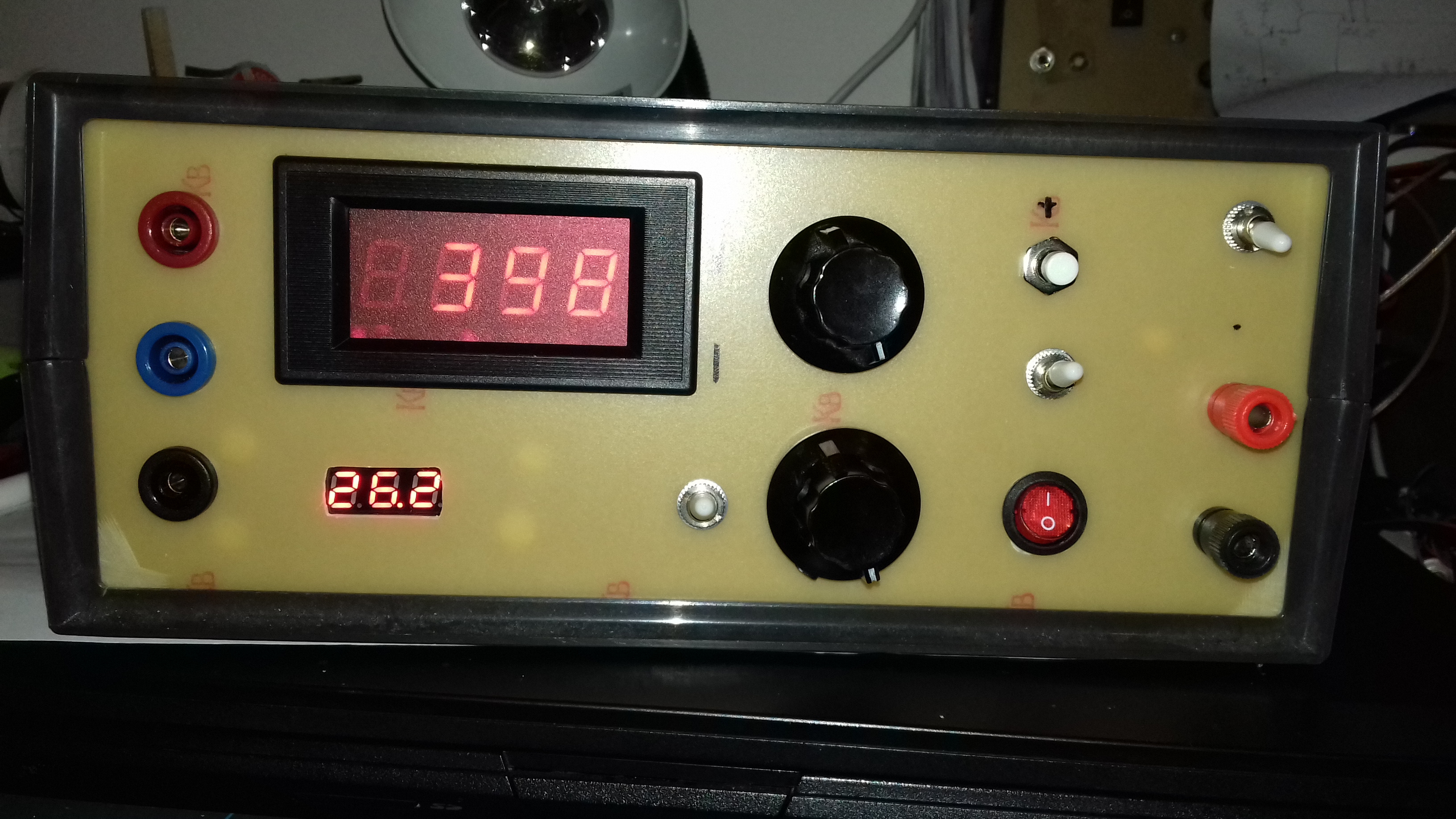
The end result:
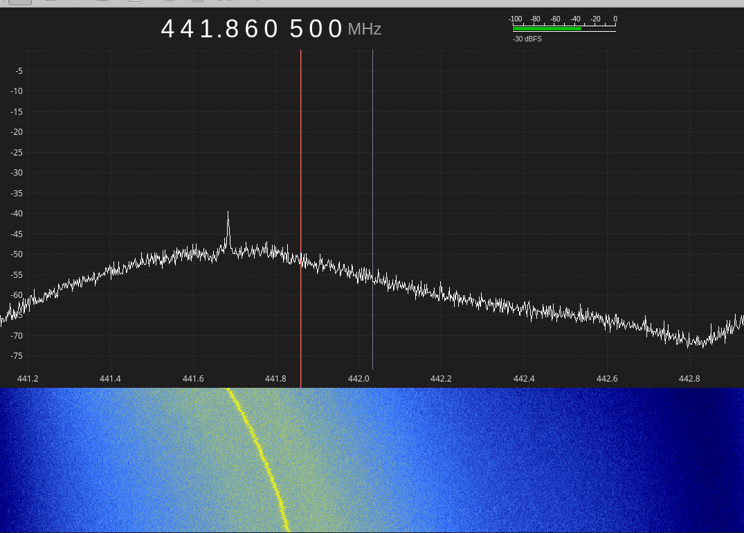
The diagram:
might need a pull down resistor on pin D5 to ground since on open air even a finger touch will make it select the TX frequency. On "0" then default to enable the RX frequency. Added an LED to be on during TX frequency select and blinking 3 times during boot. The MUX out is not needed but could be implemented on the future to check if the lock is on.
The code (will change the TX and RX frequency for my needs in the future):
Original at: https://github.com/F1CJN/ARDUINO-ADF4351-QO-100/blob/master/ADF4351_Dual_251119.ino
Bellow with changes:
///// code adf4351_dual_v1.ino
/// look for " PFDRFout=25; // Frequence de reference" if using a 10Mhz reference /// on the board
// ADF4351 with fixed frequency
// By Alain Fort F1CJN november 29,2019
// alain.fort.f1cjn@orange.fr
//
//
//
// ****************************************************** FRANCAIS *******************************************************
// Ce programme permet de programmer un ADF 4351 avec deux fréquences fixes et en utilisant une fréquence de reférence de 10 MHz.
// La premiére frequence frequence est utilisée avec un convertisseur émission (RX=0 et la seconde avec RX=1.Selection par PIN 5
// Les fréquence de sortie peuvent être modifiées aux lignes 79 et 80 en conservant le format.
// La frequence de reference peut être modidiée à la ligne ligne 70 (10MHz par défaut)
// ********************************************* HARDWARE IMPORTANT *******************************************************
// Avec un Arduino UN0 : utilise un pont de résistances pour réduire la tension, MOSI (pin 11) vers
// ADF DATA, SCK (pin13) vers CLK ADF, Select (PIN 3) vers LE
// Resistances de 560 Ohm avec 1000 Ohm à la masse sur les pins 11, 13 et 3 de l'Arduino UNO pour
// que les signaux envoyés DATA, CLK et LE vers l'ADF4351 ne depassent pas 3,3 Volt.
// Pin 2 de l'Arduino (pour la detection de lock) connectee directement à la sortie MUXOUT de la carte ADF4351
// La carte ADF est alimentée en 5V par la carte Arduino (les pins +5V et GND sont proches de la LED Arduino).
// ***********************************************************************************************************************
//
//
// *************************************************** ENGLISH ***********************************************************
// This software is used to programm an ADF4351 with Two fixed frequency, using a 10 MHz reference frequency.
// The frequency can be changed at lines 79 and 80, using the same format.Frequency selection is done with Arduino PIN 5.
// The reference frequency can be changed at line 70, using the same format (Default 10 MHz)
// ******************************************** HARDWARE IMPORTANT********************************************************
// With an Arduino UN0 : uses a resistive divider to reduce the voltage, MOSI (pin 11) to
// ADF DATA, SCK (pin13) to ADF CLK, Select (PIN 3) to ADF LE
// Resistive divider 560 Ohm with 1000 Ohm to ground on Arduino pins 11, 13 et 3 to adapt from 5V
// to 3.3V the digital signals DATA, CLK and LE send by the Arduino.
// Arduino pin 2 (for lock detection) directly connected to ADF4351 card MUXOUT.
// The ADF card is 5V powered by the ARDUINO (PINs +5V and GND are closed to the Arduino LED).
#include <SPI.h>
#define ADF4351_LE 3
uint32_t registers[6] = {0x4580A8, 0x80080C9, 0x4E42, 0x4B3, 0xBC803C, 0x580005} ; // 437 MHz avec ref à 25 MHz
//uint32_t registers[6] = {0x3D88FA8, 0x8009F41, 0x14E42, 0x4B3, 0x91003C, 0x580005} ; // 1969,501 MHz avec ref à 10 MHz
//uint32_t registers[6] = {0, 0, 0, 0, 0xBC803C, 0x580005} ; // 437 MHz avec ref à 25 MHz
int address,modif=0;
unsigned int i = 0;
double FreqTX, FreqRX, RFout, REFin, INT, PFDRFout, OutputChannelSpacing, FRACF;
double RFoutMin = 35, RFoutMax = 4400, REFinMax = 250, PDFMax = 32;
unsigned int long RFint,RFintold,INTA,RFcalc,PDRFout, MOD, FRAC;
byte OutputDivider;byte lock=2; byte RX=1;
unsigned int long reg0, reg1;
void WriteRegister32(const uint32_t value) //Programme un registre 32bits
{
digitalWrite(ADF4351_LE, LOW);
for (int i = 3; i >= 0; i--) // boucle sur 4 x 8bits
SPI.transfer((value >> 8 * i) & 0xFF); // décalage, masquage de l'octet et envoi via SPI
digitalWrite(ADF4351_LE, HIGH);
digitalWrite(ADF4351_LE, LOW);
}
void SetADF4351() // Programme tous les registres de l'ADF4351
{ for (int i = 5; i >= 0; i--) // programmation ADF4351 en commencant par R5
WriteRegister32(registers[i]);
}
//************************************ Setup ****************************************
void setup() {
Serial.begin (9600); // Serial to the PC via Arduino "Serial Monitor" at 9600
pinMode(2, INPUT); // PIN 2 en entree pour lock
pinMode(5, INPUT); // Pin 5 for TX/RX
pinMode(ADF4351_LE, OUTPUT); // Setup pins
digitalWrite(ADF4351_LE, HIGH);
SPI.begin(); // Init SPI bus
SPI.setDataMode(SPI_MODE0); // CPHA = 0 et Clock positive
SPI.setBitOrder(MSBFIRST); // poids forts en tête
PFDRFout=25; // Frequence de reference
RFintold=1234;//pour que RFintold soit different de RFout lors de l'init
RFout = RFint/100 ; // fréquence de sortie
OutputChannelSpacing = 0.005; // Pas de fréquence min
//******************************************************
FreqTX=1969.501;
FreqRX=51.8462;
//******************************************************
RX=1; //
// ct2gqv
pinMode(6, OUTPUT); // PIN 6 for display if on tx and blink 3 times during boot.
digitalWrite(6, HIGH); delay(500); digitalWrite(6, LOW); delay(500);
digitalWrite(6, HIGH); delay(500); digitalWrite(6, LOW); delay(500);
digitalWrite(6, HIGH); delay(500); digitalWrite(6, LOW);
} // Fin setup
void loop()
{
//**********************************************
RX = digitalRead(5); // reading RX/TX
if (RX==0){RFout=FreqTX; digitalWrite(6, HIGH);} // output frequency selection // ct2gqv put out 6 high to display we are in tx
if (RX==1){RFout=FreqRX; digitalWrite(6, LOW);} // output frequency selection // ct2gqv put out 6 high to low since we are in rx
RFint=RFout;
//********************************************
if (RFint != RFintold) {
if (RFout >= 2200) {
OutputDivider = 1;
bitWrite (registers[4], 22, 0);
bitWrite (registers[4], 21, 0);
bitWrite (registers[4], 20, 0);
}
if (RFout < 2200) {
OutputDivider = 2;
bitWrite (registers[4], 22, 0);
bitWrite (registers[4], 21, 0);
bitWrite (registers[4], 20, 1);
}
if (RFout < 1100) {
OutputDivider = 4;
bitWrite (registers[4], 22, 0);
bitWrite (registers[4], 21, 1);
bitWrite (registers[4], 20, 0);
}
if (RFout < 550) {
OutputDivider = 8;
bitWrite (registers[4], 22, 0);
bitWrite (registers[4], 21, 1);
bitWrite (registers[4], 20, 1);
}
if (RFout < 275) {
OutputDivider = 16;
bitWrite (registers[4], 22, 1);
bitWrite (registers[4], 21, 0);
bitWrite (registers[4], 20, 0);
}
if (RFout < 137.5) {
OutputDivider = 32;
bitWrite (registers[4], 22, 1);
bitWrite (registers[4], 21, 0);
bitWrite (registers[4], 20, 1);
}
if (RFout < 68.75) {
OutputDivider = 64;
bitWrite (registers[4], 22, 1);
bitWrite (registers[4], 21, 1);
bitWrite (registers[4], 20, 0);
}
INTA = (RFout * OutputDivider) / PFDRFout;
MOD = (PFDRFout / OutputChannelSpacing);
FRACF = (((RFout * OutputDivider) / PFDRFout) - INTA) * MOD;
FRAC = round(FRACF); // On arrondit le résultat
registers[0] = 0;
registers[0] = INTA << 15; // OK
FRAC = FRAC << 3;
registers[0] = registers[0] + FRAC;
registers[1] = 0;
registers[1] = MOD << 3;
registers[1] = registers[1] + 1 ; // ajout de l'adresse "001"
bitSet (registers[1], 27); // Prescaler sur 8/9
bitSet (registers[2], 28); // Digital lock == "110" sur b28 b27 b26
bitSet (registers[2], 27); // digital lock
bitClear (registers[2], 26); // digital lock
SetADF4351(); // Programme tous les registres de l'ADF4351
RFintold=RFint;//modif=0;
}
} // fin loop
//// end code
Have a nice day!